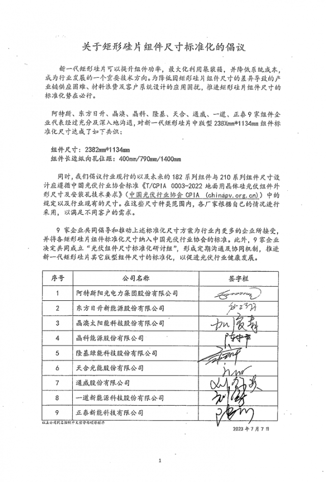
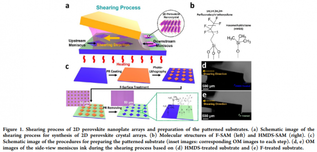
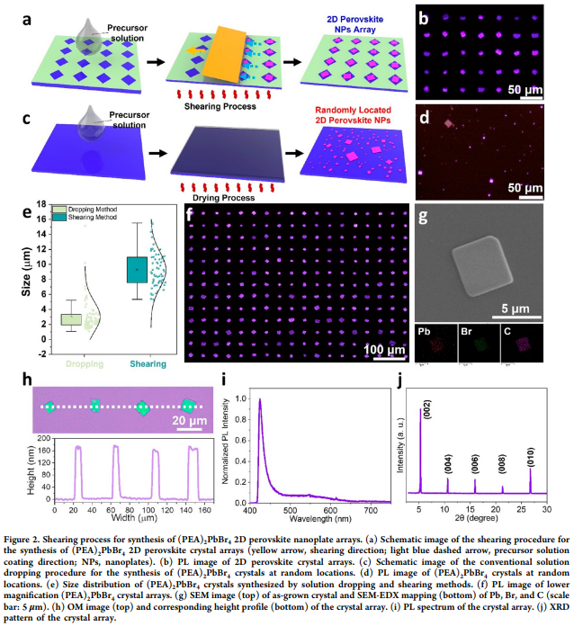
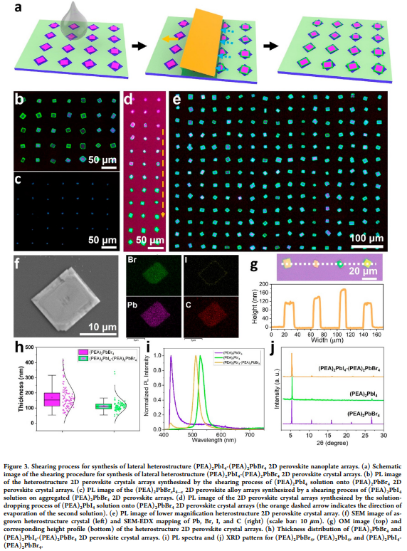
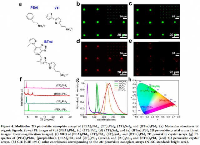

portant; overflow-wrap: break-word !important; color: rgba(0, 0, 0, 0.9); font-family: system-ui, -apple-system, BlinkMacSystemFont, "Helvetica Neue", "PingFang SC", "Hiragino Sans GB", "Microsoft YaHei UI", "Microsoft YaHei", Arial, sans-serif; font-size: 17px; font-style: normal; font-variant-ligatures: normal; font-variant-caps: normal; font-weight: 400; letter-spacing: 0.578px; orphans: 2; text-align: justify; text-indent: 0px; text-transform: none; white-space: normal; widows: 2; word-spacing: 0px; -webkit-text-stroke-width: 0px; background-color: rgb(255, 255, 255); text-decoration-thickness: initial; text-decoration-style: initial; text-decoration-color: initial;">二维钙钛矿晶体由于其优异的半导体特性而因其多样化的光电特性而引起了人们的广泛关注。然而,迄今为止的大多数研究都集中在单晶上,由于它们与选择性生长或传统光刻技术不兼容,因此对集成到器件阵列中提出了挑战。鉴于此,2023年7月11日普渡大学窦乐添portant; overflow-wrap: break-word !important; color: rgba(0, 0, 0, 0.9); font-family: system-ui, -apple-system, BlinkMacSystemFont, "Helvetica Neue", "PingFang SC", "Hiragino Sans GB", "Microsoft YaHei UI", "Microsoft YaHei", Arial, sans-serif; font-size: 17px; font-style: normal; font-variant-ligatures: normal; font-variant-caps: normal; font-weight: 400; letter-spacing: 0.578px; orphans: 2; text-align: justify; text-indent: 0px; text-transform: none; white-space: normal; widows: 2; word-spacing: 0px; -webkit-text-stroke-width: 0px; background-color: rgb(255, 255, 255); text-decoration-thickness: initial; text-decoration-style: initial; text-decoration-color: initial;">portant; overflow-wrap: break-word !important;">于ACS Nano刊发一步溶液图案化制备二维钙钛矿纳米板阵列的研究成果,提出了一种通过在图案化基底上进行弯液面引导涂层来合成二维钙钛矿晶体阵列的简便的一步解决方法。进一步利用这种方法来合成横向异质结构纳米板阵列。成功实现了六种不同的二维钙钛矿纳米板阵列,包括外延异质结构。光学和晶体学表征显示了纳米板的高光学性能和结晶度。此外,该方法还进一步用于制备高性能2D钙钛矿纳米板ink); text-decoration: none; -webkit-tap-highlight-color: rgba(0, 0, 0, 0); cursor: pointer; max-width: 100%; box-sizing: border-box !important; overflow-wrap: break-word !important;">光电传感器portant; overflow-wrap: break-word !important;">阵列。该策略可用作光学性质的基础研究和钙钛矿材料高性能光电子学(包括光电传感器和显示器)开发的指南。